
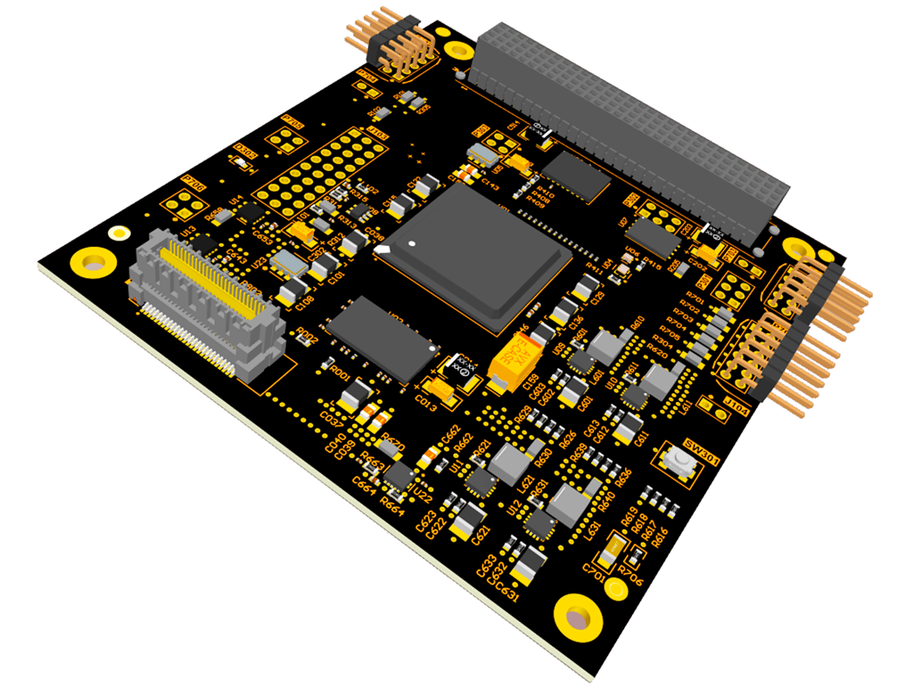
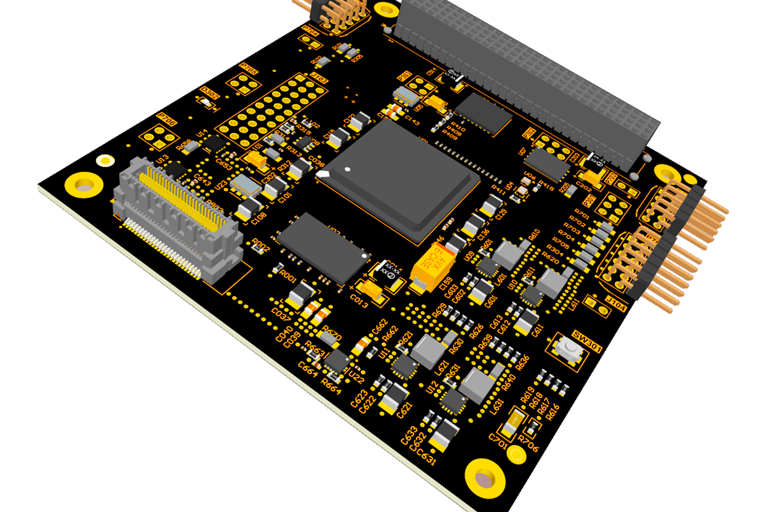
Spectra PCB
Precision Engineering for a Connected Future


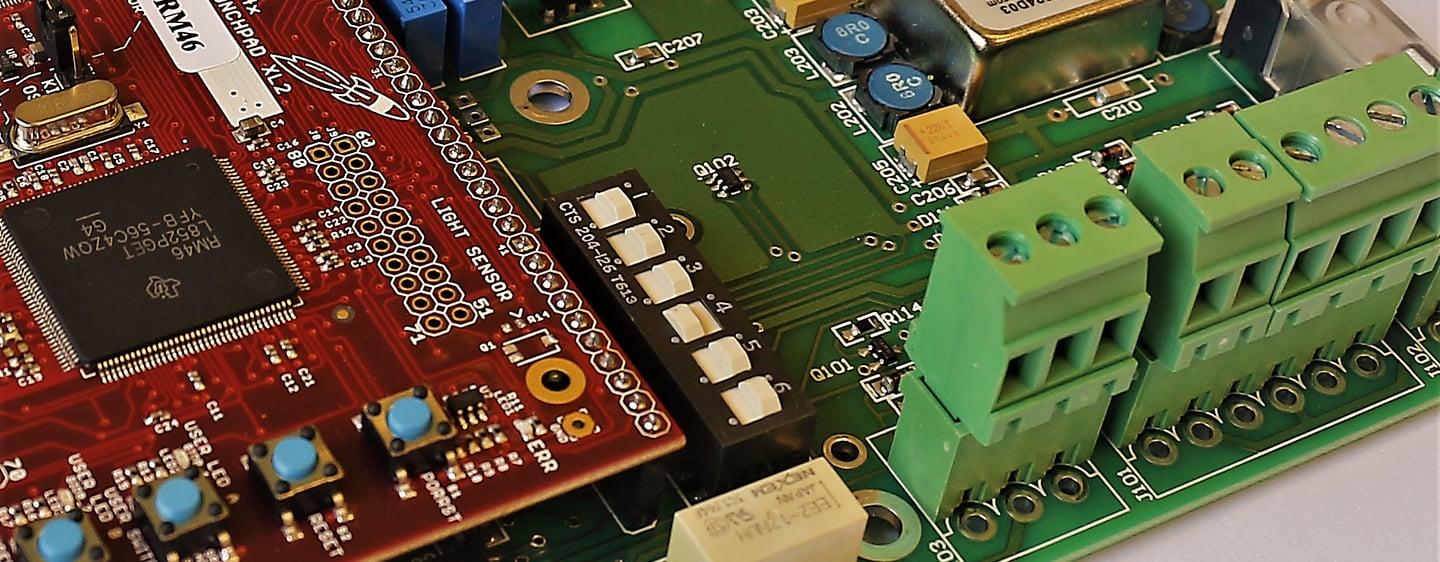
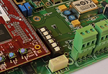
PCB & Antenna Design

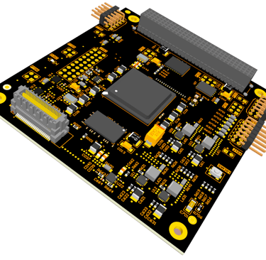
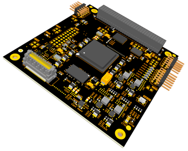
Spectra PCB
PCB & Antenna Design
Precision Engineering for a Connected Future
About Our Design Services
What We Offer
Custom PCB design using industry-leading tools
High-speed and multi-layer PCB development with optimized:
Signal integrity
Power distribution
Grounding strategies
EMI/EMC performance
Careful routing techniques for:
Controlled impedance traces
Noise reduction
Reliable analog and digital performance
Antenna Design
PCB Design
What We Offer
Custom antenna design for:
Embedded antennas
PCB antennas
Patch antennas
Dipole and monopole antennas
Directional antennas
Contact IoT antennas
Multi-band and wideband systems
RF and electromagnetic design using advanced simulation tools for:
Impedancia matching
Radiation pattern optimization
Gain and efficiency improvement
Size reduction and integration constraints
Complete hardware design support for:
FPGAs
Microcontrollers
Sensors
IoT systems
Mixed-signal electronics
Development Process
Our workflow focuses on performance, reliability, and efficient collaboration:
Optimazed component placement
Design validation and debugging
Prototype and production coordination
Collaboration with hardware, firmware, and R&D teams
Ideal For
Embedded systems
Industrial electronics
FPGA-based designs
High-speed digital systems
IoT devices
Custom electronic products
Engineering Capabilities
Multi-layer stack-up optimization
DFM-oriented design (Design for Manufacturing)
Power integrity and thermal considerations
Connector and interface integration
3D PCB visualization and mechanical verification
Cost and manufacturability optimization
Deliverables
We provide complete production-ready documentation, incluiding:
Gerber files
BOM (Bill of Materials)
Assembly documentation
Manufacturing outputs
Development for wireless technologies incluiding:
Wi-Fi
Bluetooth
LTE / 5G
GNSS / GPS
ISM bands
LoRa
RFID
Custom RF systems
Engineering Capabilities
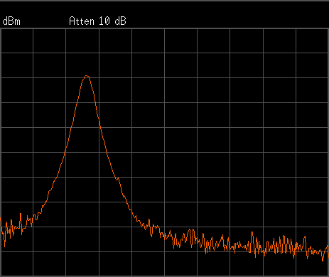
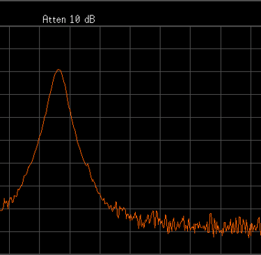
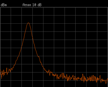
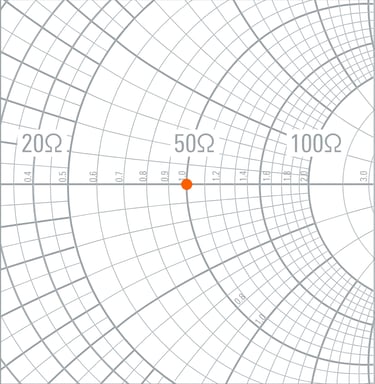
Electromagnetic simulation and optimization
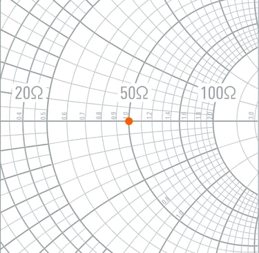
S-parameter analysis and matching networks
PCB antenna integration
Multi-layer RF PCB design
RF feed and transmission line optimization
EMI/EMC-aware RF layouts
Compact and low-profile antenna solutions
Mechanical integration support
Prototype & Validation
We support the full antenna development cycle:
Design and simulation
Prototype fabrication
Tuning and optimization
Measurement and validation
Iterative performance improvemets
Deliverables
Complete engineering documentation incluiding:
Manufacturing files
RF layout files
Simulation results
Metching network recommendations
Prototype-ready PCB data
Technical reports and performance analysis
Development Approach
Our process is focused on achieving reliable real-world RF performance while meeting mechanical and manufacturing constrints:
Application-driven antenna optimization
Collaboration with hardware and mechanical teams
Fast prototyping and interactive refinement
Performance-focused RF engineering
Ideal Applications
IoT devices
Wireless embedded systems
Industrial RF products
Telemetry and tracking systems
Wearable electronics
High-frecuency communication systems
Custom wireless hardware development


About Our Design Services
PCB Design
What We Offer
Custom PCB design using industry-leading tools
High-speed and multi-layer PCB development with optimized:
Signal integrity
Power distribution
Grounding strategies
EMI/EMC performance
Careful routing techniques for:
Controlled impedance traces
Noise reduction
Reliable analog and digital performance
Complete hardware design support for:
FPGAs
Microcontrollers
Sensors
IoT systems
Mixed-signal electronics
Engineering Capabilities
Multi-layer stack-up optimization
DFM-oriented design (Design for Manufacturing)
Power integrity and thermal considerations
Connector and interface integration
3D PCB visualization and mechanical verification
Cost and manufacturability optimization
Deliverables
We provide complete production-ready documentation, incluiding:
Gerber files
BOM (Bill of Materials)
Assembly documentation
Manufacturing outputs
Development Process
Our workflow focuses on performance, reliability, and efficient collaboration:
Optimazed component placement
Design validation and debugging
Prototype and production coordination
Collaboration with hardware, firmware, and R&D teams
Ideal For
Embedded systems
Industrial electronics
FPGA-based designs
High-speed digital systems
IoT devices
Custom electronic products
Antenna Design
What We Offer
Custom antenna design for:
Embedded antennas
PCB antennas
Patch antennas
Dipole and monopole antennas
Directional antennas
Contact IoT antennas
Multi-band and wideband systems
RF and electromagnetic design using advanced simulation tools for:
Impedancia matching
Radiation pattern optimization
Gain and efficiency improvement
Size reduction and integration constraints
Development for wireless technologies incluiding:
Wi-Fi
Bluetooth
LTE / 5G
GNSS / GPS
ISM bands
LoRa
RFID
Custom RF systems
Engineering Capabilities
Electromagnetic simulation and optimization
S-parameter analysis and matching networks
PCB antenna integration
Multi-layer RF PCB design
RF feed and transmission line optimization
EMI/EMC-aware RF layouts
Compact and low-profile antenna solutions
Mechanical integration support
Prototype & Validation
We support the full antenna development cycle:
Design and simulation
Prototype fabrication
Tuning and optimization
Measurement and validation
Iterative performance improvemets
Deliverables
Complete engineering documentation incluiding:
Manufacturing files
RF layout files
Simulation results
Metching network recommendations
Prototype-ready PCB data
Technical reports and performance analysis

Development Approach
Our process is focused on achieving reliable real-world RF performance while meeting mechanical and manufacturing constrints:
Application-driven antenna optimization
Collaboration with hardware and mechanical teams
Fast prototyping and interactive refinement
Performance-focused RF engineering
Ideal Applications
IoT devices
Wireless embedded systems
Industrial RF products
Telemetry and tracking systems
Wearable electronics
High-frecuency communication systems
Custom wireless hardware development
Crafting Innovative Circuit Solutions
At SpectraPCB, we specialize in advanced antenna, RF circuit, and PCB design solutions, delivering high-performance engineering for the aerospace, nuclear, electronics, and IoT industries with precision and engineering excellence.
150+
15+
Years of Experience
Successful Projects Delivered
Engineering Expertise
We bring experience in the nuclear and aerospace industries, developing high-reliability PCB, RF, and antenna solutions for demanding environments.


Connect
Get in Touch with us
Explore
Innovate
+54 9 221 419 5777
© 2026. All rights reserved.