Circuit Design Services
Offering modern and elegant solutions for aerospace, nuclear, electronics, and IoT industries.
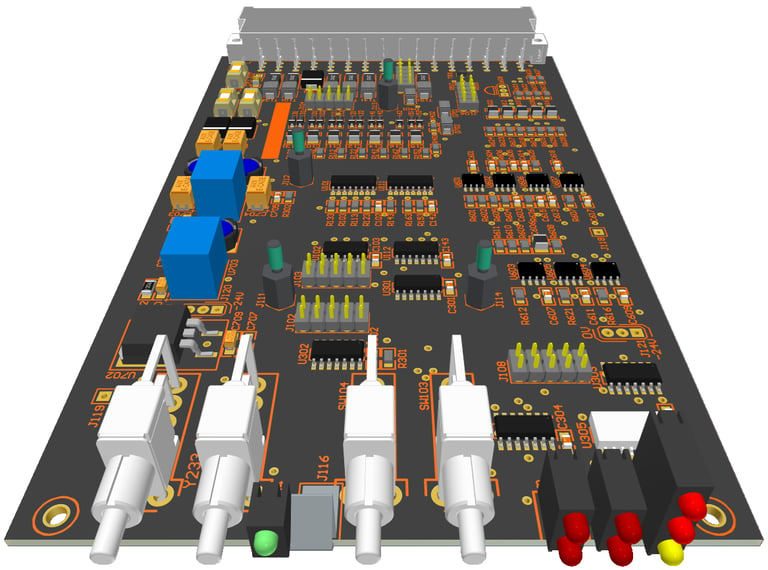
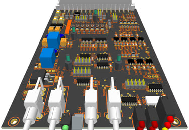
Advanced Digital Circuit
High-speed digital design for FPGA and DDR systems.
Advanced Analog Circuit
Low-noise analog and RF circuit design.
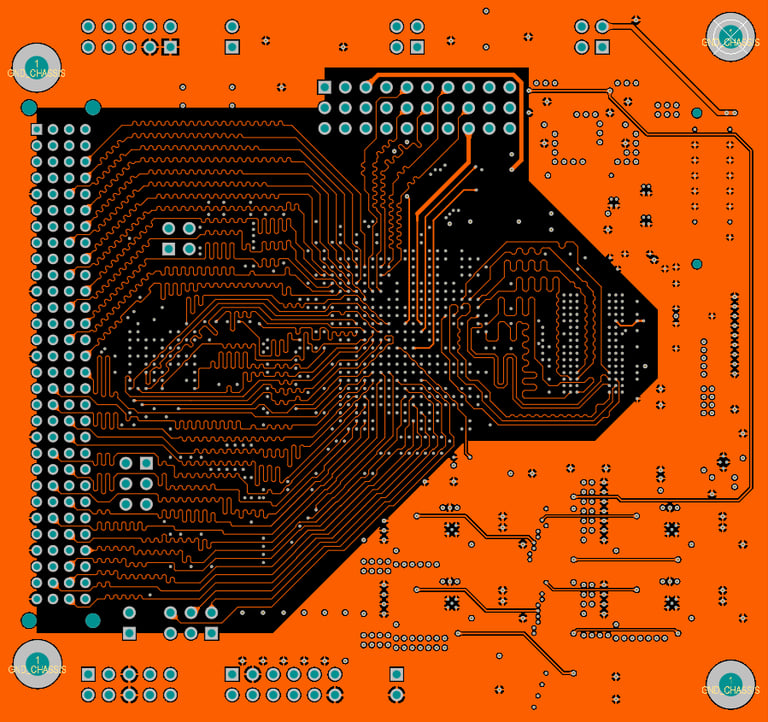
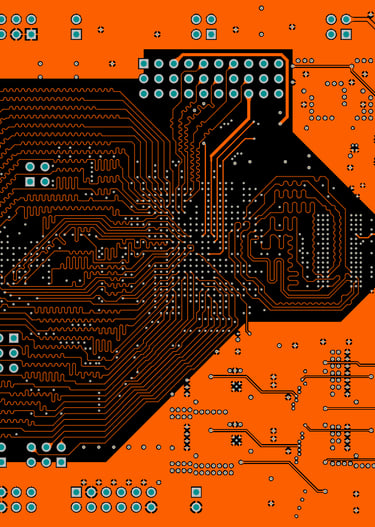
Controlled-impedance multilayer PCB routing.
Precision PCB Routing
Technical highlights
Expertise in PCB design using Altium Designer and KiCad
Careful signal routing with controlled trace widths and minimized noise
Strong analog and digital electronics design knowledge
Multi-layer stack-up development for improved grounding and power integrity
PCB optimization focused on cost, performance, and manufacturability
Delivery of Gerber files, BOMs, fabrication outputs, and full documentation
EMI/EMC-aware design practices with signal integrity and power management considerations
Experience designing systems with FPGAs, microcontrollers, sensors, and IoT devices
DFM-oriented layouts for reliable manufacturing and assembly
Connector integration and flexible interface implementation
3D PCB visualization for mechanical fit verification and assembly validation


Design approach
Optimized component placement to reduce signal path lengths and improve performance
Mixed-signal layout techniques to minimize interference and coupling noise
Collaboration with hardware, firmware, and R&D teams throughout development
PCB validation, testing support, and debugging assistance
Coordination with PCB manufacturers and assembly vendors for prototyping and production
Experience delivering high-speed and complex multi-layer PCB designs
Connect
Get in Touch with us
Explore
Innovate
+54 9 221 419 5777
© 2026. All rights reserved.